Discover our complete solutions portfolio covering Cathodic Protection and Corrosion management - PCB design and plating - Functional and decorative plating - Electrocoating - Acoustics
Discover Protect
Elsyca V-PIMS
A revolution in digital PIMS combining Pipeline Corrosion Integrity Management System (PIMS) and computational modeling capabilities
Elsyca IRIS
Deep analysis of AC threats supporting efficient mitigation systems computer-aided design
Elsyca CatPro
Graphical simulation platform for cathodic protection and DC stray current analysis of pipeline networks
Elsyca CPManager
3D CAD-based software simulation platform for the computer-aided design and analysis of cathodic protection installations
Elsyca ACTA
Unique solution offering accurate, disambiguated, and tailored risk ranking report of pipeline networks
Plate
Elsyca PlatingManager
Leverage a digital twin of your plating line to predict plating performance and increase manufacturing capacity
Elsyca PCBBalance
The world’s only PCB DFM software that applies automated and optimized copper balancing to your PCB design and panel layout.
Elsyca PCBPlate
State-of-the-art graphical simulation platform for enhancing the plating performance of your PCB panel and pattern plating processes.
Elsyca ECoatMaster
CAD independent software platform for the simulation of the automotive electrocoating process of a body-in-white (BIW).
Elsyca EPOS
Simulate the performances of electropolishing processes based on a virtual mock-up of the electropolishing cell.
Elsyca AnodizingManager
State-of-the-art graphical simulation platform for analyzing the production performance and quality of anodizing processes.
Innovate
Elsyca CorrosionMaster
CorrosionMaster identifies corrosion hot spots and predicts corrosion rates, enabling engineers to look at alternative material combinations and/or coating systems, or investigate corrosion-mitigating measures.
Elsyca LeakageMaster
Improve vehicles interior acoustic comfort by performing upfront virtual smoke tests.
Elsyca MeshingMaster
Automatically creates meshes for a variety of applications such as acoustics, CFD, thermal analysis, etc
Elsyca XPlorer
Interactive simulation results viewer for Finite Elements results
Elsyca XPlorer3D
Analyze, Understand and Get Immersed in your results
Elsyca PCBPlate
Accelerate optimization of production configuration
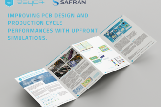
More infoDownload White Paper
Contact us 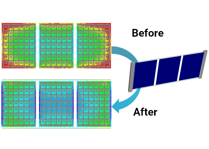
Key Benefits
Quality
Visualize the risk zones (out-of-spec layer thickness) on all areas of all panels – including all your test coupons. Find out all relevant key performance indicators to each individual board on the entire flight bar.
Time-to-Market
The fill production set-up including panel layout can be optimized long before the first production run. Avoid expensive trial-and-error runs and stressful production surprises. Buy yourself some peace of mind.
Profit margins
Avoid trial runs and reduce plating problems without the necessity for increasing plating times, ... it all leads to higher profits for your company.
Knowledge
Elsyca PCBPlate is an investment in knowledge as it helps to accumulate and store critical company know-how. All experiments can be done on the digital twin of your plating line, in a no-risk environment for your production.
Customer satisfaction
Become a value-adding partner for your customer. Advice your customer on DFM. Build up knowledge by using intelligent simulation software and enhance your overall service level.

Key features
A wide range of functionalities
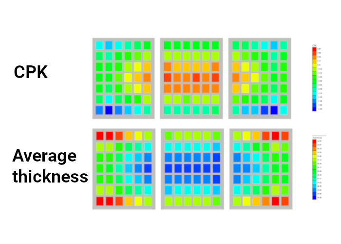
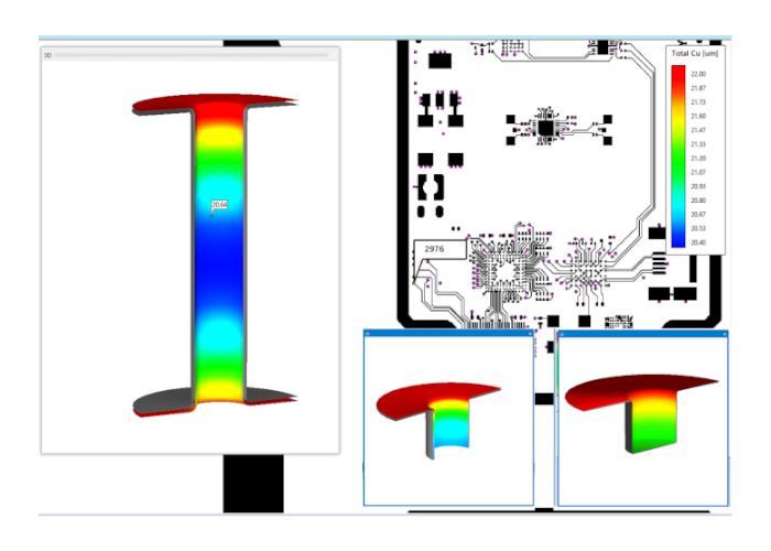
Identify layer thickness distribution over boards and panels
Generate color plots of layer thickness distribution and related production risk zones inside the holes and over the boards and panels.
Produce 2D bar charts for efficient production variance analysis.
Own a digital twin of your specific plating infrastructure
Your real-life plating tanks, including their particular plating chemistry, are pre-configured in your installed version of the Elsyca PCB software, resulting in very accurate simulation results.
Total quality control
Full view on quality hotspots before the first part is built. KPI information is available for all PCBs on the production configuration. Physical test coupon measurements can be used as a benchmark for simulation results in all other areas.

Easily incorporate PCB layout information
Ask your colleagues from the CAM department to export the PCB layout in Extended Gerber format (available in almost every CAM package) and import it directly into the Elsyca PCBPlate database.
Support full panel history
Compute the total layer thickness distribution over the panel, while accounting for the full panel history: position of the panel on the flight bar and process parameters for each plating step, as well as other relevant steps like etching or electroless deposition
Optimization in just a few iterations
Easy what-if simulation to verify the impact of layout modifications, tooling (shielding, current robbers, or even auxiliary anodes), different panel configurations and loads (and thus production capacity) and process parameter modifications.
Convenient to share and collaborate
Elsyca PCBPlate supports the free standalone Elsyca XPlorer viewer, the visualization and post-processing environment that allows sharing color plot results with other stakeholders.
Automated yet customizable reports
Automated yet customizable reports are generated at the end of the simulation process, in support of ISO quality processes


 versus surface area in this range (Y-axis)")


")
Elsyca PCBPlate is a state-of-the-art PCB plating simulation platform providing detailed layer thickness distribution information over the panels, patterns and inside holes.
To ensure the simulation results provide accurate and reliable information, a validation study was executed on panels produced by Eurocircuits (www.eurocircuits.com). The setup was a combination of different boards on a panel, in a 2x2 panel layout.
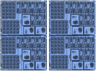
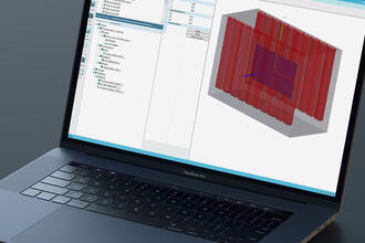
Fig1: panel layout flightbar
Different measurement points were defined on the front/back side of the panels as well as areas of interest for through-holes.
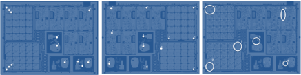
Fig 2: location measurement points front side/back side and area holes front side
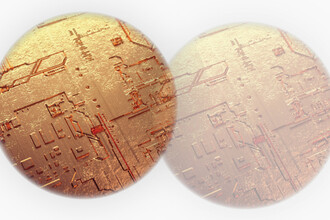
The layer thickness distribution was computed for all panels, what follows are the simulation and measurement results of the panel at the upper right position on the flight bar.
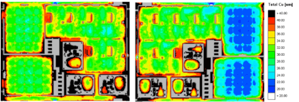
Fig 3: front side on the left, back side on the right
The maximum/minimum layer thickness values where measured inside the holes in the selected areas, and compared with the simulation results. The results are shown in the graph below.
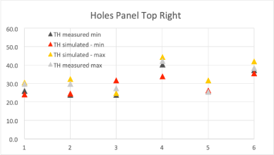
Summarizing the measured/simulated maximum/minimum values in the holes:
| Minimum Value | Maximum Value | |
| Average measured thickness | 29.5 | 32.4 |
| Average simulated thickness | 29.4 | 34.4 |
| Deviation | -0.4% | 5.9% |
Next, the values at the pre-defined measurement points were compared:
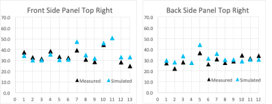
summarizing the measured/simulated values on the panel/pattern:
| Front Side | Back Side | |
| Average measured thickness | 33.6 | 29.8 |
| Average simulated thickness | 36.1 | 32 |
| Deviation | 7.4% | 7.2% |
Conclusion
The validation study proves the software provides a +90% accuracy level for the simulated layer thickness value. This implies the Elsyca PCBPlate users can rely on the simulation results to upfront validate the different design, panel layout or process configurations.